Circuits and Electronics
Table of Contents
- 1 Introduction
- 2 Intro to Circuits and Electronics
- 3 Ohms Law
- 4 KVL KCL
- 5 Common Circuitry
- 6 Node and Mesh Analysis
- 7 Thevenin and Norton
- 8 Source transform
- 9 Superposition
- 10 Diodes
- 11 Operational Amplifier (Op Amp)
- 12 DC and AC Signal Analysis
- 12.2 AC (Small Signal) Analysis
- 13 Metal Oxide Field Effect Transistor (MOSFET)
- 14 Bipolar Junction Transistor (BJT)
- 15 Negative Feedback Amplifier
1 Introduction
Recommended resources:
Online public textbooks: All About Circuits
(Paid) Textbook: Sedra Smith Microelectronic Circuits
2 Intro to Circuits and Electronics
3 Ohms Law
| Quanity | Symbol | Unit of Measurement |
|---|---|---|
| Current | I | Ampere (A) |
| Voltage | V | Volt (V) |
| Resistance | R | Ohm (Ω) |
- The unit of resistance is ohms (1Ω = V/A).
- Ohm's law says that the current through a conductor is given by the following; $I = \frac{V}{R}$.
- Where V is the voltage across a conductor.
4 KVL KCL
4.1 Kirchhoff’s Voltage Law (KVL)
4.1.1 In a Series Circuit
- The algebraic sum of all voltages in loop must equal zero.
- $V_{total} = V_{1} + V_{2} + V_{3} + ...V_{n}$.
4.1.2 In a Parallel Circuit
- The voltage across every resistor is the same as the supply voltage.
- $V_{total} = V_{1} = V_{2} = V_{3} = ...V_{n}$.
4.2 Kirchhoff's Current Law (KCL)
4.2.1 In a Parallel Circuit
- The algebraic sum of all currents entering and exiting a node must equal zero.
- The total current in a parallel circuit must equal the sum of the branch
currents.
- $I_{in} = I_{out}$.
5 Common Circuitry
5.1 Voltage Divider
WIP.
5.2 Current Divider
WIP.
5.3 Delta Wye
WIP.
6 Node and Mesh Analysis
WIP.
7 Thevenin and Norton
Conversions:
- $R_{Th} = R_{N}$.
- $V_{Th} = I_{N} \times R_{N}$.
- $I_{N} = \frac{V_{Th}}{R_{Th}}$.
7.1 Thevenin
Voltage source series to resistor.
7.2 Norton
Current source parallel to resistor.
8 Source transform
WIP.
9 Superposition
WIP.
10 Diodes
Shockley diode equation: $I_{D} = I_{S} \left( e^{\frac{V_{D}}{nV_{T}}} - 1 \right)$.
- $I_{D}$ = Diode current.
- $I_{S}$ = Reverse bias saturation current.
- $V_{D}$ = Voltage across the diode.
- $V_{T}$ = Thermal voltage.
-
Where $V_{T} = \frac{kT}{q}$.
$k$ = Boltzmann constant.- $T$ = Absolute temperature $K$.
- $q$ = Magnitude of an electron's charge, aka elementary charge $C$.
-
$n$ = Ideality / quality factor or emission coefficient.
11 Operational Amplifier (Op Amp)
11.1 Gain
Gain: $A = \frac{output}{input}$.
Voltage gain: $A_{v} = \frac{v_{output}}{v_{input}}$.
12 DC and AC Signal Analysis
12.1 DC Analysis
Important aspects to remember:
- Signal / AC sources are short.
- Coupling / decoupling / bypass capacitors are open.
12.2 AC (Small Signal) Analysis
Important aspects to remember:
- DC sources are short.
- Coupling / decoupling / bypass capacitors are short.
- Transistors (BJT, MOSFET, etc.) operate to their small signal model.
- Transistors require bias currents to find small signal model parameters.
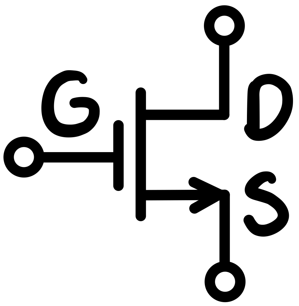
13 Metal Oxide Field Effect Transistor (MOSFET)
For an ideal MOSFET, the gate current is essentially zero. The gate is insulated from the channel by a thin layer of oxide, and no direct current flows through the gate. This insulation makes the MOSFET a voltage-controlled device.
Therefore, the current relationship in an NMOS under normal operation, assuming no substrate (body) current, is $I_{D} = I_{S}$, since $I_{G} = 0$.
MOSFETs are driven by current as its control signal input.
13.1 Operating Mode / Response Region
| NPN Configuration | Input | Control Signal Input | Output |
|---|---|---|---|
 |
Drain | Gate | Source |
| Operating Mode | Characteristics | Application |
|---|---|---|
| Cutoff | $v_{GS} < V_{t}$ | Digital 0 |
| Triode | $v_{GD} > V_{t}$ or $v_{OV} > V_{DS}$ | Digital 1 |
| Saturation | $v_{GD} \leq V_{t}$ or $v_{OV} \leq V_{DS}$ | Amplifier |
- $V_{t}$ = Threshold voltage.
- $V_{OV}$ = Over voltage, $V_{OV} = v_{GS} - V_{t}$.
13.2 I-V Relationship
| Operating Mode | I-V relationship |
|---|---|
| Cutoff | $i_{D} = 0$ |
| Triode | $i_{D} = k_{n}' \frac{W}{L} \left( \left( v_{GS} - V_{t} \right) v_{DS} - \frac{1}{2} v^{2}_{DS} \right)$ |
| Saturation | $i_{D} = \frac{1}{2} k_{n}' \frac{W}{L} \left( v_{GS} - V_{t} \right)^{2}$ |
- Where $k_{n}' = \mu_{n} C_{ox}$ and $k_{n} = k_{n}' \frac{W}{L}$.
- $\mu_{n}$ = Electronic mobility of N-type $Cm^2 / Vs$.
- $C_{ox}$ = Oxide capacitance $fF / \mu m^{2}$.
- $W$ = Channel width.
- $L$ = Channel length.
13.3 Small Signal Analysis (AC)
Signal model parameters:
$g_{m} = \frac{2 I_{D}}{V_{OV}}$.
13.3.1 T Model & Hybrid Pi Model
Dependant current: $i_{D} = g_{m} v_{GS}$.
Resistance: $r_{o} = \infty$.
13.4 Amplifier Applications
Recall, the MOSFET must operate in saturation mode.
| Common Source | Common Source with Source Resistor | Common Gate | Common Drain | |
|---|---|---|---|---|
| Model | Hybrid Pi | T | T | T |
| Input | Gate | Gate | Source | Gate |
| Output | Drain | Drain | Drain | Source |
| $R_{in}$ | $\infty$ | $\infty$ | $g_{m}^{-1}$ | $\infty$ |
| $R_{out}$ | $R_{D}$ | $R_{D}$ | $R_{D}$ | $g_{m}^{-1}$ |
| Voltage gain, $A_{v}$ | $-g_{m} \left( R_{D} \vert \vert R_{L} \right)$ | $\frac{-g_{m} \left( R_{D} \vert \vert R_{L} \right)}{1 + R_{S}} - \frac{R_{D} \vert \vert R_{L}}{g_{m}^{-1} R_{S}}$ | $g_{m} \left( R_{D} \vert \vert R_{L} \right)$ | $\frac{R_{L}}{g_{m}^{-1} + R_{L}}$ |
14 Bipolar Junction Transistor (BJT)
BJTs are driven by voltage as its control signal input.
14.1 Operating Mode / Response Region
| NPN Configuration | Input | Control Signal Input | Output |
|---|---|---|---|
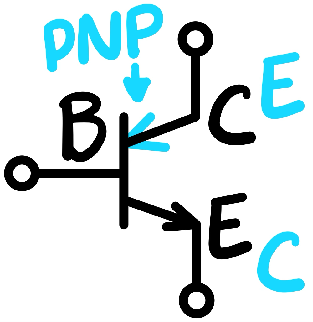 |
Collector | Base | Emitter |
| Operating Mode | EB Junction | CB Junction | Characteristics | ~BE Voltage | ~BC Voltage | Application |
|---|---|---|---|---|---|---|
| Cutoff | Reverse | Reverse | $V_{C} > V_{B}$ and $V_{E} > V_{B}$ | $V_{BE} < 0.5 \ \mathrm{V}$ | $V_{BC} < 0.4 \ \mathrm{V}$ | Digital 0 |
| Active | Forward | Reverse | $V_{C} > V_{B} > V_{E}$ | $V_{BE} = 0.7 \ \mathrm{V}$ | $V_{BC} < 0.4 \ \mathrm{V}$ | Amplifier |
| Saturation | Forward | Forward | $v_{B} > V_{C}$ and $V_{B} > V_{E}$ | $V_{BE} = 0.7 \ \mathrm{V}$ | $V_{BC} > 0.4 \ \mathrm{V}$ | Digital 1 |
14.2 Small Signal Analysis (AC)
Signal model parameters:
$g_{m} = \frac{I_{C}}{V_{T}}$.
14.2.1 T Model
Dependant current: $i_{C} = \alpha i_{E}$.
BE voltage: $v_{BE} = i_{E} r_{e}$.
Resistance: $r_{e} = \frac{\alpha}{g_m} = \frac{V_{T}}{I_{E}}$.
14.2.2 Pi Model
Dependant current: $i_{C} = \beta i_{B}$.
BE voltage: $v_{BE} = i_{B} r_{\pi}$.
Resistance: $r_{\pi} = \frac{\beta}{g_{m}} = \frac{V_{T}}{I_{B}}$.
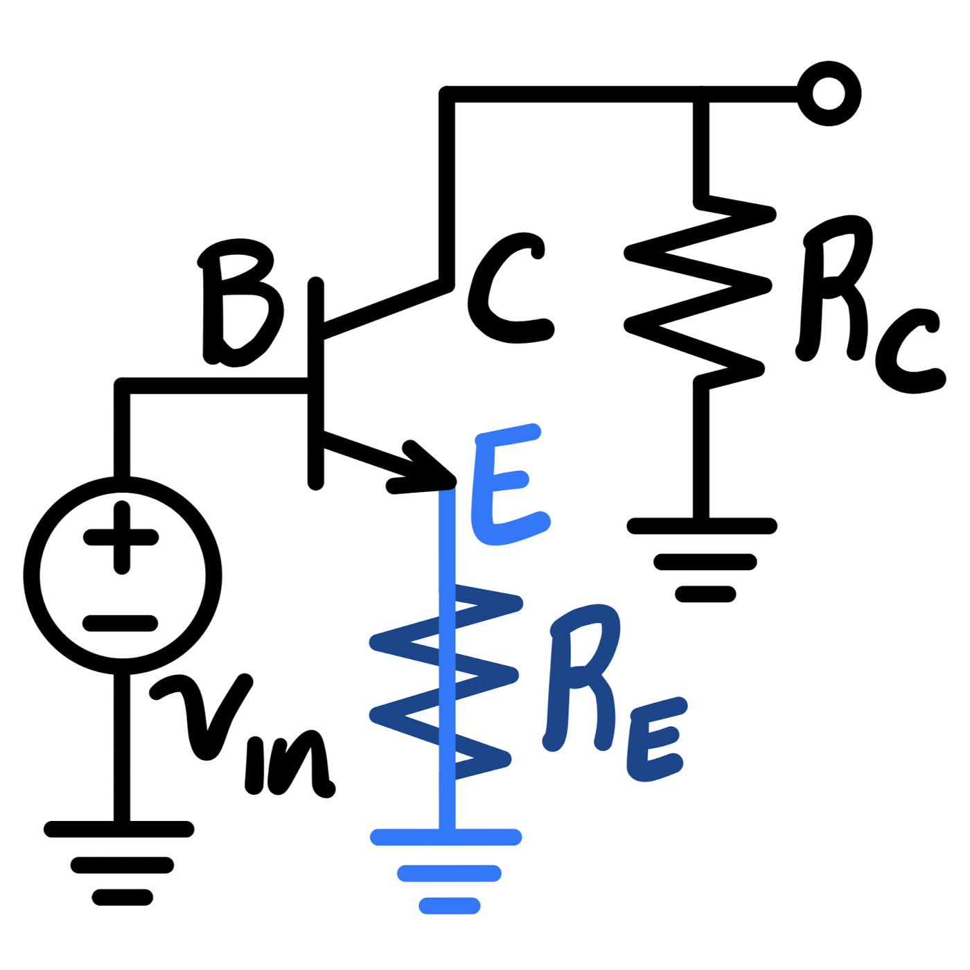
14.3 Amplifier Applications
Recall, the BJT must operate in active mode.
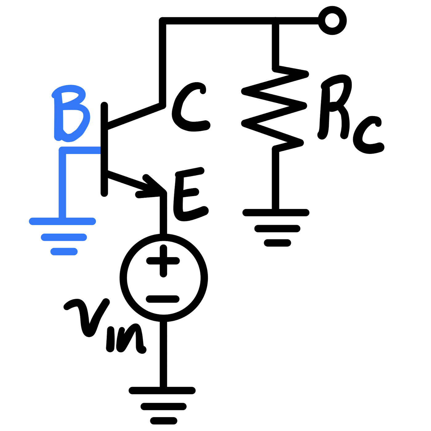
| Common Emitter | Common Emitter with Emitter Resistor | Common Base | Common Collector / Emitter Follower | |
|---|---|---|---|---|
| Circuit | 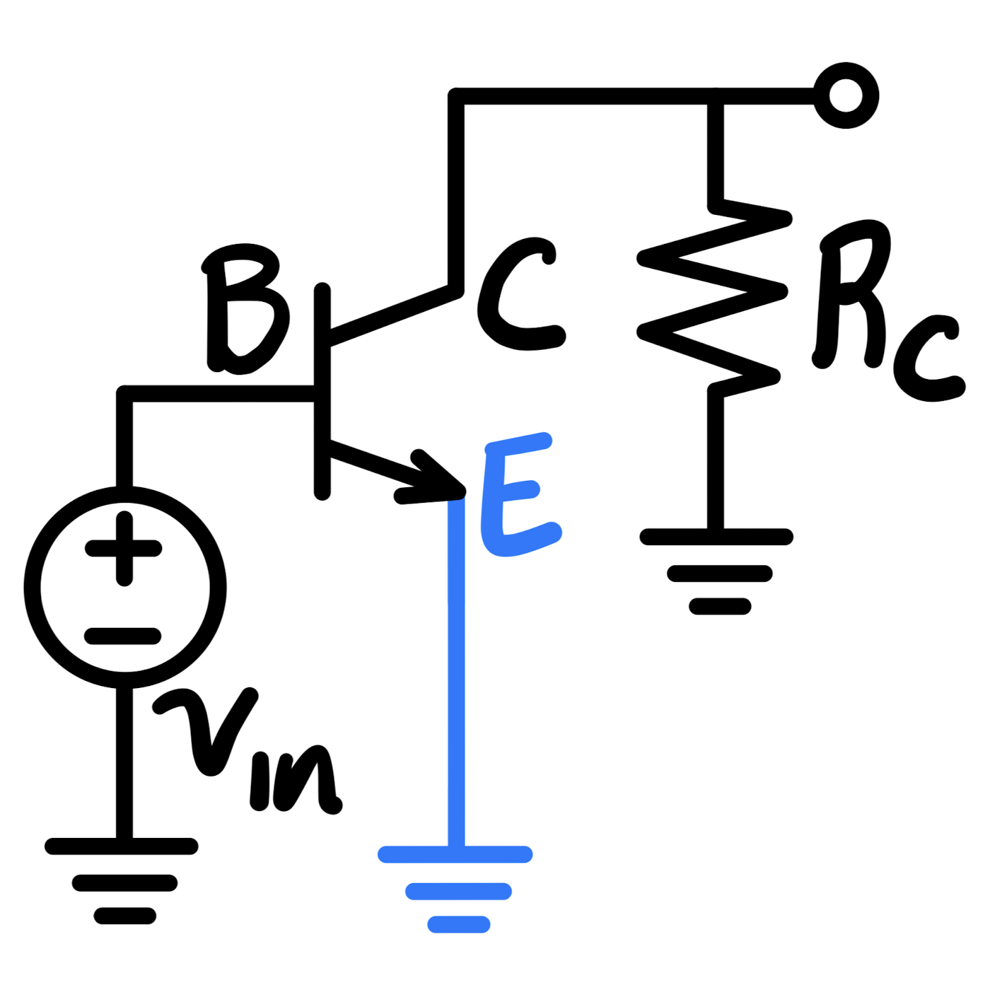 |
 |
 |
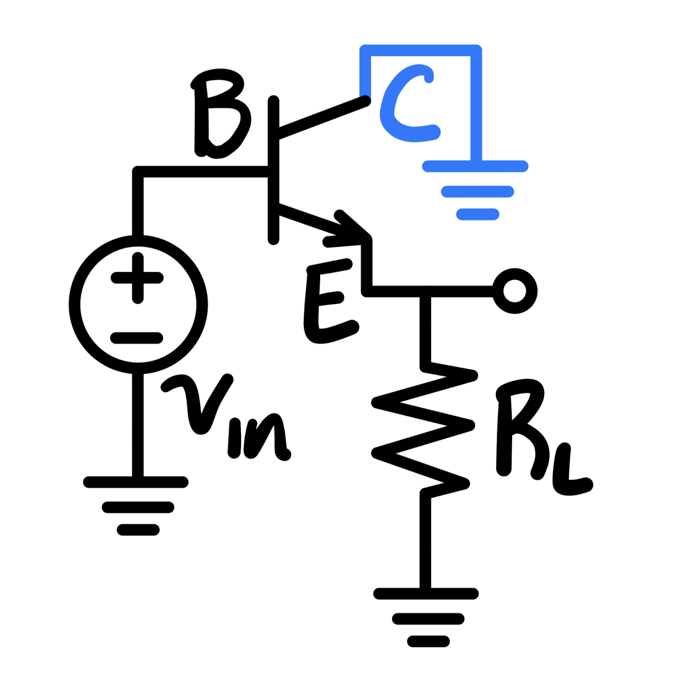 |
| Model | Pi | T | T | T |
| Input | Base | Base | Emitter | Base |
| Output | Collector | Collector | Collector | Emitter |
| $R_{in}$ | $r_{\pi}$ | $\left( 1 + \beta \right) \left( r_{e} + R_{E} \right)$ | $r_{e}$ | $\left( 1 + \beta \right) \left( r_{e} + R_{L} \right)$ |
| $R_{out}$ | $R_{C} = \frac{v_{o}}{i_{o}}$ | ← | ← | $r_{e}$ |
| Voltage gain, $A_{v_{o}}$ (no $R_{L}$) | $-g_{m} R_{C} = \frac{- \alpha R_{C}}{r_{e}}$ | $\frac{-g_{m} R_{C}}{1 + g_{m} R_{E}} = \frac{- \alpha R_{C}}{r_{e} + R_{E}}$ | $g_{m} R_{C} = \frac{\alpha R_{C}}{r_{e}}$ | 1 |
| Voltage gain, $A_{v}$ with $R_{L}$ | $A_{v_{o}}$ where $R_{C} \rightarrow \left( R_{C} \vert \vert R_{L} \right)$ | ← | ← | $\frac{R_{L}}{R_{L} + r_{e}}$ |
| Overall gain, $G_{v}$ | $\frac{R_{in}}{R_{in} + R_{sig}} \times A_{v}$ | ← | ← | ← |
Recommended video:
15 Negative Feedback Amplifier
The following information is more specific to BJT negative feedback amplifier circuits, however the main concepts carry over to other types of transistors.
| Voltage | Trans-conductance | Current | Trans-resistance | |
|---|---|---|---|---|
| Input | Voltage | Voltage | Current | Current |
| Output | Voltage | Current | Current | Voltage |
| Topology | Series-Shunt | Series-Series | Shunt-Series | Shunt-Shunt |
| Feedback network $R_{1}$, $R_{2}$ |  |
 |
 |
|
| Feedback factor $\beta$ | $\frac{V_{f}}{V_{o}} \big\vert_{I_{1} = 0}$ | $\frac{I_{f}}{V_{o}} \big\vert_{I_{1} = 0}$ | $\frac{I_{f}}{I_{o}} \big\vert_{V_{1} = 0}$ | $\frac{I_{f}}{V_{o}} \big\vert_{V_{1} = 0}$ |
| Open loop gain $A$ | Per amplifier stage based on $R_{i}$ & $R_{o}$ | ← | ← | ← |
| Feedback loop gain $A_{f}$ | Total of amplifier stages' gain | ← | ← | ← |
| Series Side Equation | Shunt Side Equation | |
|---|---|---|
| Feedback resistance, $R_{if}$ & $R_{of}$ | $\left( 1 + A \beta \right) R_{\left( i \ \mathrm{or} \ o \right)}$ | $\frac{R_{\left( i \ \mathrm{or} \ o \right)}}{ 1 + A \beta }$ |
| Input output resistance $R_{i}$, $R_{o}$ (no $R_{L}$ & $R_{sig}$) | $R_{ \left( i \ \mathrm{or} \ o \right) \ f} - R_{\left( sig \ \mathrm{or} \ L \right)}$ | $\left( R_{ \left( i \ \mathrm{or} \ o \right) \ f}^{-1} - R_{\left( sig \ \mathrm{or} \ L \right)}^{-1} \right)^{-1}$ |
Recommended video: